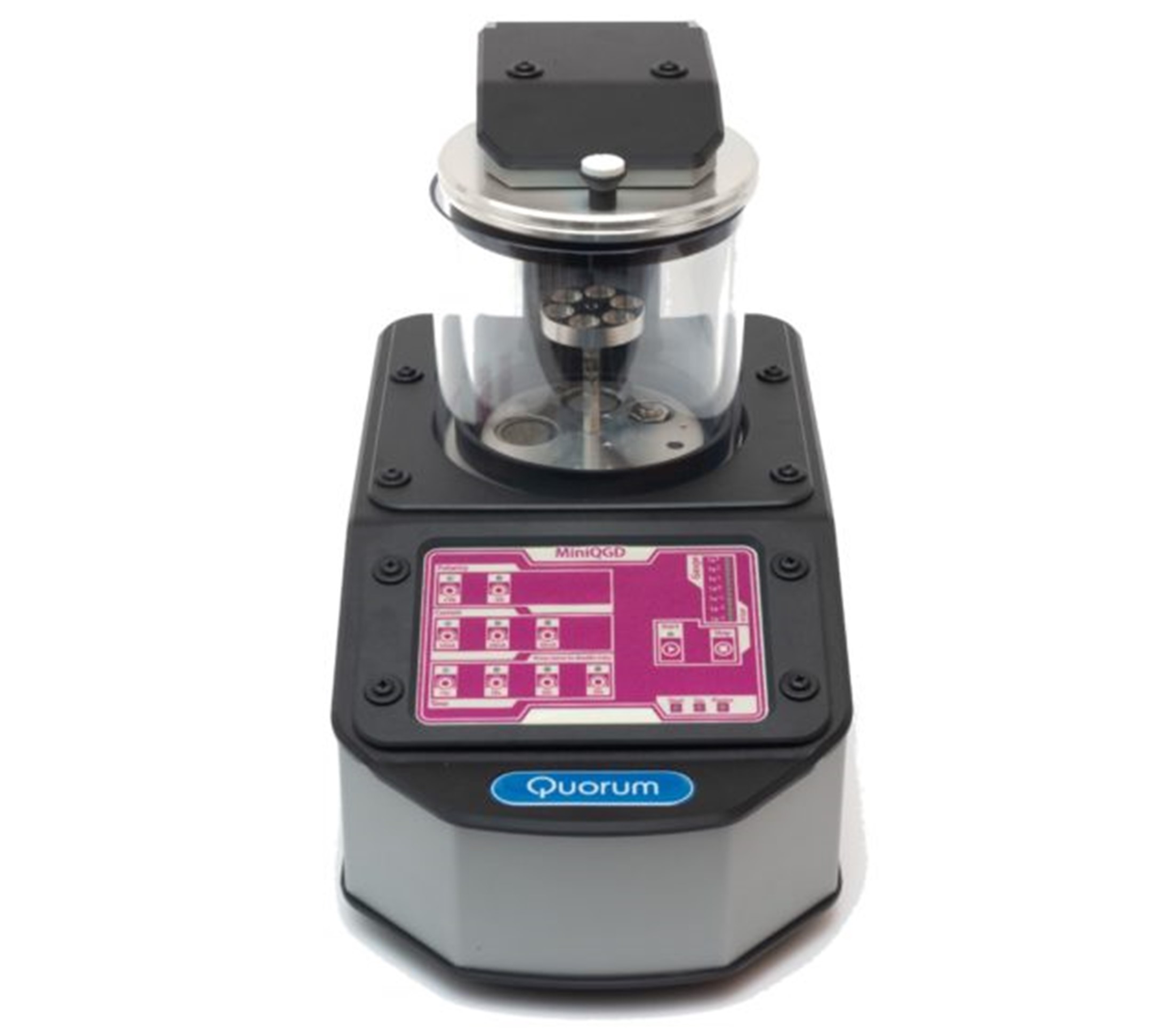
QDry
Sécheur à point critique automatique

Système FIB-SEM pour une véritable analyse structurelle en 3D
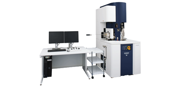
The newly developed FIB-SEM system from Hitachi, the NX9000 incorporates an optimized layout for true high-resolution serial sectioning to tackle the latest demands in 3D structural analysis and for TEM and 3DAP analyses.
The NX9000 FIB-SEM system allows the highest precision in material processing for a wide range of areas relating to advanced materials, electronic devices, biological tissues, and a multitude of other applications.
Ion milling and observation at normal incidence in real-time for true analytical imaging
The SEM column and FIB column are orthogonally arranged to realize normal incident SEM imaging of FIB cross sections.
Orthogonal column arrangement eliminates aspect deformation, foreshortening of cross-sectional images, and shift of the field of view (FOV) during serial section imaging, which cannot be avoided by conventional FIB-SEM systems.
The NX9000 images enable highly accurate 3D structural analysis. Optical correlative microscopy can be applied easily due to the benefit of surface-planar EM imaging.
Cut&See
Cut & See supports high-resolution, high-contrast imaging of biological tissues, semiconductors, and magnetic materials, such as steel and nickel, at low accelerating voltages.
Serial section images can be collected with high throughput due to the proper geometry of the ion and electron column.
3D-EDS*1
Serial section SEM images and serial section elemental maps can be collected using 3D-EDS.
The large-area silicon drift detector reduces the acquisition time and enables elemental mapping at low accelerating voltages.
3D-EBSD*1
Simultaneous SEM, FIB, and EBSD signals are obtained for 3D-EBSD without moving the stage during FIB sectioning and EBSD analysis. Accuracy and throughput of 3D crystal orientation analysis and segmentation yield high quality and less post-processing correction.